Description
Ion implantation, similar to coating process, is a high technology approach for modifying surface properties of materials. But it does not involve the addition of a layer on the surface. Ion implantation is originally developed for semiconductor applications, and it uses highly energetic beams of ions (positively charged atoms) to modify surface structure and chemistry of materials at low temperature. Certainly, such process does not adversely affect component dimensions or bulk material properties.
Application
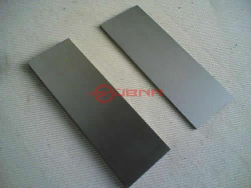
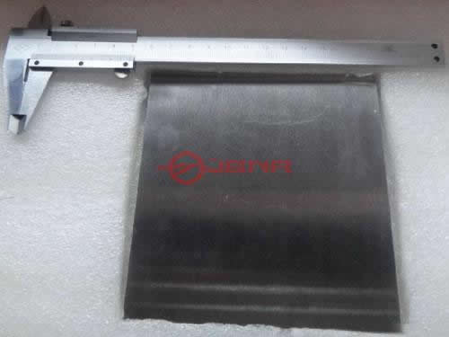
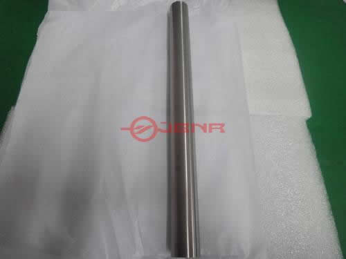
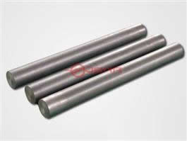
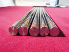
1. Featuring high thermal conductivity, material strength, corrosion resistance and absolute purity, our tungsten alloys and molybdenum alloys work well, ensuring that the ions are generated efficiently and free from impurities.
2. In ion implantation equipment, tungsten alloys and molybdenum alloys are widely used for arc chambers, filaments, cathodes and other spare parts.
Principle
The ion implantation process is often conducted in a vacuum chamber at very low pressure (10-4 to 10-5 torr). Large numbers of ions (typically 1016 to 1017 ions/cm2) bombard and penetrate a surface, interacting with the substrate atoms immediately beneath the surface. The interactions of the energetic ions with the material modify the surface, providing it with different properties other than the remainder of the material.
Founded in 2008, TallKee Refractory metals is a professional manufacturer and supplier of tungsten, molybdenum, and tantalum and niobium products in China. Having passed ISO9001-2008 international quality administrative system certification, our products like tungsten alloys and molybdenum alloys are exported to United States, South Korea, Russia, Japan, Germany, France, Brazil, Ukraine, Italy and other international markets.